Introduction
Research on semiconductor photoelectrodes developed rapidly from the 1970s. Early examples included TiO₂ photoelectrolysis with hydrogen evolution at a platinum counter electrode, and regenerative cells such as CdSe/polysulfide/metal systems. Investigating new photosensitive materials led to electrochemical methods for estimating bandgap, flat-band potential and donor or acceptor density. This article retains historical experiments and explains their analysis, with corrections to equations and limitations.
Illumination and calibration
The working electrode must be illuminated with white or monochromatic light. For wavelength-dependent measurements, place a monochromator between the broad-spectrum source and cell.
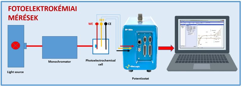
Xenon and halogen lamps cover the visible region; halogen emission also extends strongly into the infrared. The original article’s source-spectrum illustrations are retained:

Xenon-lamp illustration source.
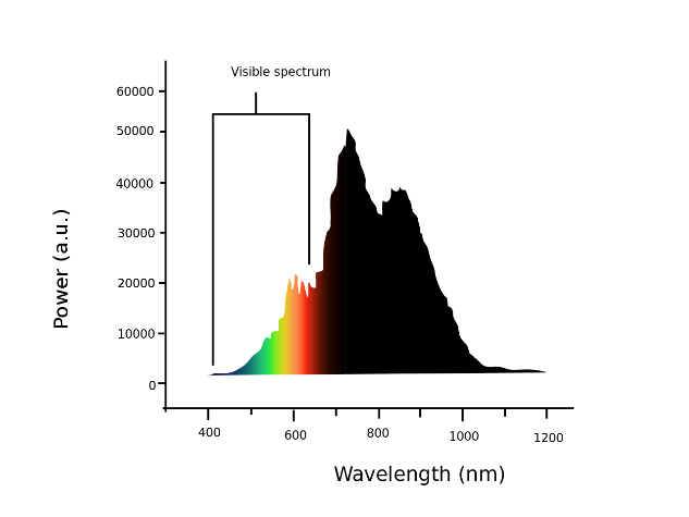
Halogen-spectrum illustration source.

A monochromator narrows the spectral band, but scattered light and higher diffraction orders may require additional filtering. Calibrate irradiance at every wavelength, at the electrode position and with the same optical path. Account for detector spectral response, cell windows and electrolyte absorption.
Entrance and exit slit widths control spectral bandwidth and available power. Narrower slits improve spectral discrimination but reduce photocurrent; select and record a workable compromise.
Photoelectrochemical cell and potentiostat
A photoelectrochemical cell has an optical window giving access to the working electrode. UV measurements require a window material with suitable transmission, commonly appropriate quartz; ordinary glass or plastics may absorb the required wavelengths.
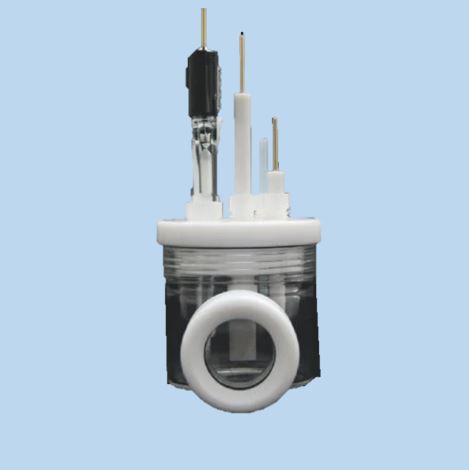
Many cell geometries are available. Match optical access, electrode mounting and electrolyte compatibility to the experiment.
Potentiostat requirements depend on expected photocurrent, background, capacitance and time resolution. The original article mentioned approximately 0.1–100 µA with 0.001 µA resolution and an EIS span from 10 µHz to 1 MHz. These are historical examples, not universal minimum specifications. Programmable polarisation scans are also useful.
Capacitance–potential measurements can support Mott–Schottky analysis when capacitance can reasonably be assigned to the space-charge region. Helmholtz capacitance, surface states, frequency dependence and series resistance can distort the result. A straight line alone does not establish an accurate donor density. BioLogic AN24 illustrates EC-Lab analysis.
Calculating quantum efficiency
Incident photon-to-current efficiency, IPCE, is the ratio of collected photogenerated electrons to incident photons. Subtract dark current at the same potential. Let jph be photocurrent density and Pλ irradiance, normalised to the same area:
- Ne/A = |jph|t/qe, with qe = 1.602176634 × 10⁻¹⁹ C.
- Eλ = hν = hc/λ, with h = 6.62607015 × 10⁻³⁴ J·s and c = 299,792,458 m/s.
- Nph/A = Pλt/Eλ. Pλ is power per area, not energy; use W/cm² with A/cm², for example.
- IPCE = (Ne/A)/(Nph/A) = |jph|hc/(qeλPλ). Multiply by 100 for percent.
Time cancels. The old article inverted this ratio and mixed cm² and m²; these are the corrected expressions.
Our illustrative calculation: at 500 nm, 1.00 mW/cm² and 0.100 mA/cm² photocurrent density, IPCE ≈ 24.8%. Resolve area normalisation if illuminated and active areas differ.
Repeat at different wavelengths to obtain a spectrum. IPCE is an external efficiency based on incident photons. Absorbed photon-to-current efficiency, APCE, additionally requires absorption/reflection information. Proper absolute optical calibration permits absolute IPCE; unknown optical losses do not automatically yield an absolute or internal efficiency.
Semiconductor concepts
The bandgap separates conduction- and valence-band edges:
Eg = Ec − Ev. (5)
For the simple band-to-band excitation picture, photon energy must reach the gap: hν ≥ Eg (6). Direct and indirect transitions differ; the latter also involve momentum transfer.
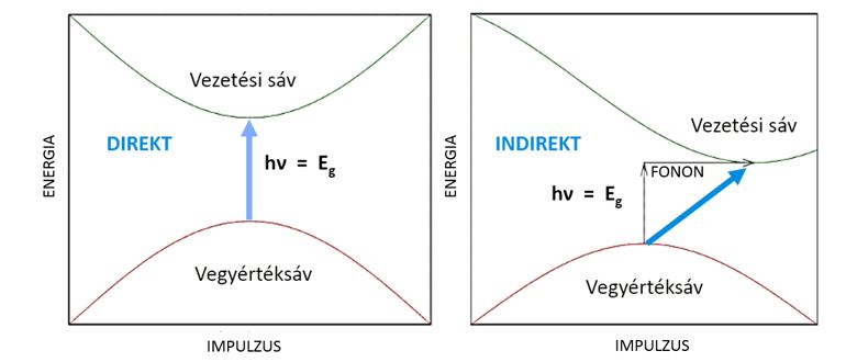
Near an idealised allowed band edge, write αhν = A(hν − Eg)^(n/2) (7), with a material- and transition-dependent prefactor A. Here n = 1 denotes an allowed direct transition and n = 4 an allowed indirect transition. This model is not valid for every material or across an entire spectrum. α has units of inverse length; 1/α is the absorption length.
Semiconductor–electrolyte interface and photocurrent
Under appropriate anodic polarisation and interface conditions, an n-type semiconductor can form a depleted space-charge region of thickness W. In a simple absorption model, with reflection treated separately:
Φ(x) = Φ(0)exp(−αx); G(x) = αΦ(0)exp(−αx). (8)
Φ is photon flux; G is generation per volume and time. They are different quantities. At x = 1/α, flux has fallen to 1/e of its surface value; this is not a sharp cutoff for absorption or carrier generation.
In the depletion region, the electric field can direct holes toward the semiconductor–solution interface, where oxidation occurs. Minority carriers generated outside that region may also reach it by diffusion. Their diffusion length is denoted Lp in the model below.
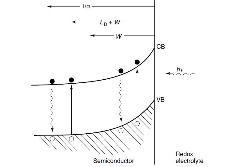
The retained interface diagram is attributed in the original article to Krishnan Rajeshwar, Fundamentals of Semiconductor Electrochemistry and Photoelectrochemistry (original linked copy).
The Gärtner model gives:
ηλ = 1 − exp(−αW)/(1 + αLp). (9)
It assumes ideal collection within the depletion region. Reflection, surface recombination and slow interfacial transfer require separate treatment. The original theoretical source is Gärtner, Physical Review 116, 84–87 (1959).
In the depletion approximation:
W = √[2εsVsc/(qeNd)]. (10)
εs is absolute permittivity, εrε0; Vsc is the positive magnitude of the depletion-region potential drop. For an n-type electrode, the conventional anodic direction gives approximately Vsc = V − Vfb when potentials share a reference and Helmholtz changes are negligible. State the sign convention and any thermal correction used.
Rearranging gives:
−ln(1−η) = ln(1 + αLp) + α√[2εsVsc/(qeNd)]. (11)
Plot −ln(1−η) against √Vsc. The slope is α√[2εs/(qeNd)] and intercept ln(1+αLp). With reliable absolute η and known Nd, α and Lp can be estimated; assess the uncertainty of the extrapolated intercept. Conversely, known α can support an Nd estimate under the same assumptions.
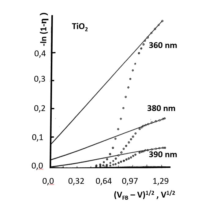
The original author’s TiO₂ single-crystal example used 1 N H₂SO₄ and reported Lp = (2.1 ± 0.8) × 10⁻⁵ cm and Nd = 9 × 10¹⁶ cm⁻³. The archived discussion associated agreement with approximately 1–2 V polarisation. Lower-potential departures may involve recombination, Helmholtz potential changes or slow reaction kinetics. This is a historical interpretation, not an independently revalidated measurement. There is no universal 1 V threshold for Gärtner applicability.
Historical spectral example: Cd₄SiSe₆ and Cd₄GeSe₆
The original author describes work published as Kovach, S.K., Motrja, S.F., Semrad, E.E., Photoelectrochemical Properties of Cd₄SiSe₆ and Cd₄GeSe₆, Elektrokhimiya 28 (1992), 1000–1005. The optical properties of these then relatively new materials motivated the study.
Electrodes were prepared from approximately 4 × 4 × 5 mm single crystals, polished with parallel faces. A natural crystal face contacted the solution; copper wire was attached to the back using indium. Epoxy insulated the contacts and side faces. Exposed area, approximately 10–20 mm², was measured microscopically.
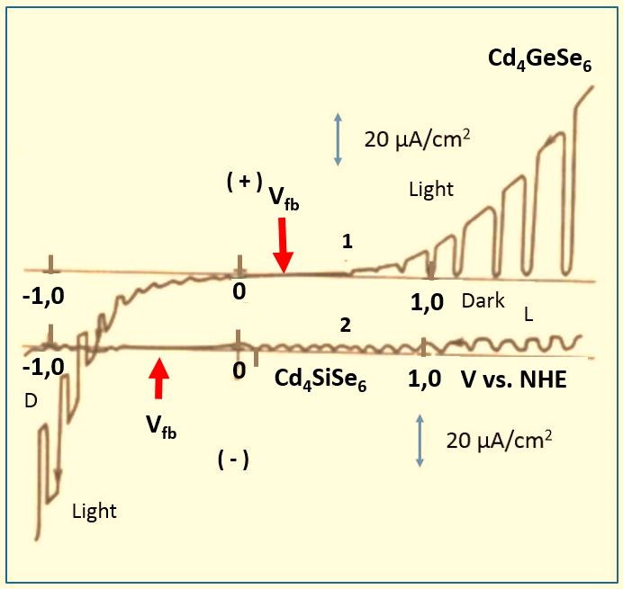
Archived polarisation curves: Cd₄GeSe₆ (1) and Cd₄SiSe₆ (2), 0.05 M H₂SO₄, scan rate 20 mV/s, chopped monochromatic illumination at 620 nm. Dark and illuminated intervals reveal the photoresponse.
Anodic photocurrent often occurs for an n-type photoanode in depletion; cathodic photocurrent can occur for a p-type photocathode. Dark current also depends on redox chemistry, surface states and contacts. Current onset or sign reversal does not universally locate Vfb or establish conductivity type. Independent analysis is needed. The archived interpretation describes both materials as n-type, with Cd₄SiSe₆ closer to highly resistive behaviour.
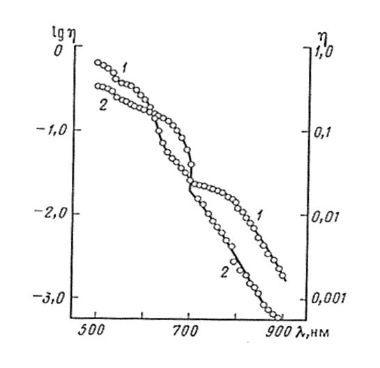
The original relative spectra vary by roughly three orders of magnitude. Features were discussed near 540, 640 and 700 nm for Cd₄SiSe₆ and near 540 and 700 nm for Cd₄GeSe₆, with weaker response beyond 700 nm.
When αLp ≪ 1, checked over the analysed range, the model gives:
−ln(1−η) ≈ α(Lp + W) = α′. (12)
At fixed potential, W is treated as constant. Combining with the band-edge model:
(α′hν)^(2/n) = const × (hν − Ei). (13)
Ei is the extrapolated transition energy. Plot both (α′hν)² and (α′hν)^(1/2) against hν, examining justified linear regions. Sparse data can make the interpretation ambiguous.
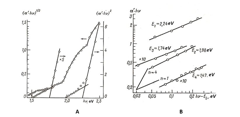
The original Cd₄SiSe₆ comparison uses two representations. In the stated convention, n = 1 means direct, not indirect as an old sentence said. Taking logarithms gives:
log(α′hν) = const + (n/2)log(hν − Ei). (14)
The fitted slope can test consistency with the selected exponent but does not independently prove a transition assignment.
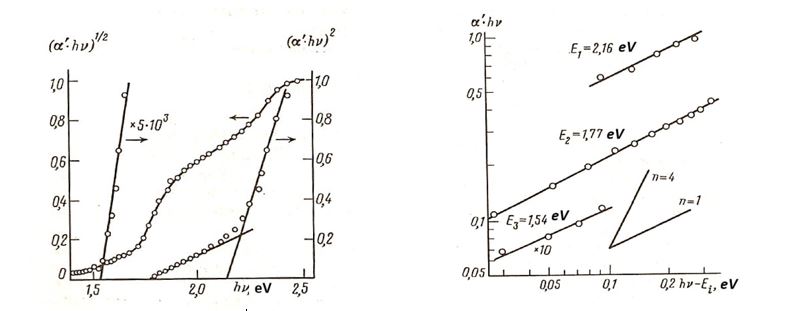
The last figure is the corresponding Cd₄GeSe₆ analysis; its previous repeated Cd₄SiSe₆ caption has been corrected. Historical reported energies were 1.47 ± 0.02, 1.74 ± 0.02, 1.97 ± 0.02 and 2.24 ± 0.02 eV for Cd₄SiSe₆; and 1.54 ± 0.02, 1.77 ± 0.02 and 2.16 ± 0.02 eV for Cd₄GeSe₆.
The author later reported a photoluminescence comparison for Cd₄GeSe₆: S. Kovách, Á. Nemcsics, Z. Lábadi, S. Motrya, Investigation of the Electronic Structure of Cd4GeSe6 by Photoelectrochemical and Photoluminescence Methods, Inorganic Materials 39 (2003), 108–112. These historical claims were not experimentally revalidated for this revision.
Interpretation limits and records
Photoelectrochemistry can constrain bandgap, flat-band potential, doping and spectral response when its assumptions are justified. An arbitrarily normalised relative spectrum cannot be inserted as absolute η into −ln(1−η). Collection, recombination and reaction kinetics influence the shape as well as absorption.
Retain raw dark/light currents, irradiance calibration, spectral bandwidth, reference electrode, area definition and fitting intervals. A straight transformed segment alone is not proof of transition type. Related local guide: EIS data quality.